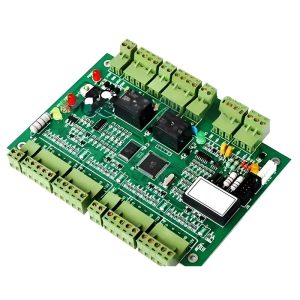
PCB Assembly
As leading one-stop PCB Assembly services provider in China, AVPCB offers high quality, cost effective and express PCB board products and provides PCB manufacturing, electronics assembly manufacturing, components sourcing, Box build assembly and PCBA testing services for our customers.
For full turn-key circuit board assembly, we take care of the entire process, including Printed Circuit Boards fabrication, components sourcing, order tracking, continuous monitoring of quality and final PCB board assembly. Whereas for partial turn-key, the customer can provide the PCBs and certain components, and the remaining parts will be handled by us.
PCB Assembly Types We Offer
-
Turnkey PCB Assembly – We handle everything from PCB fabrication to component procurement and assembly.
-
Consigned and Partial Turnkey Assembly – Use your own components or let us supply the rest.
-
Prototyping to Mass Production – Flexible volumes with rapid prototyping available.
-
Single or Double-sided SMT and Through-hole Assembly
-
Mixed Technology Assembly (SMT + THT)
Why Choose AVPCB for Your PCBA Needs?
-
ISO9001 & RoHS Certified Manufacturing
-
Long-term partnerships with Digikey, Mouser, and other authorized suppliers
-
Fast response, flexible production, and strict quality control
-
Free DFM/DFA feedback and stencil service for new orders
-
Excellent customer support and after-sales service
Through a systematic PCB design and manufacturing process, our company is able to provide high-quality PCB electronic board assembly to meet the various needs of our customers. Whether it is preliminary design or large-scale production, we are committed to ensuring the success of each project. Feel free to contact us to learn more about our PCB design and manufacturing services!
Showing all 11 results
-
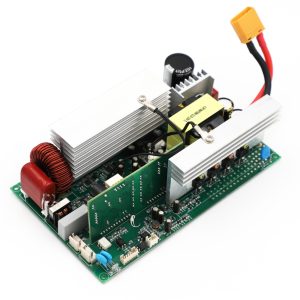
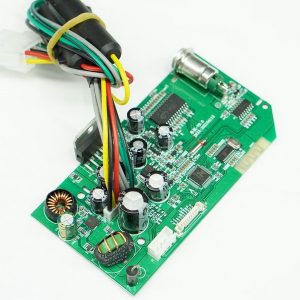
12V 24V Dc To 220V Solar Power Inverter Electronic PCB Board
Read more -
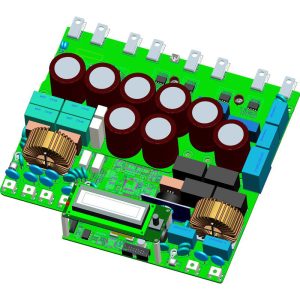
12V Dc To 220V Solar Hybrid Power Factory Original Oem Iot Inverter Electronic PCB Circuit Board
Read more -
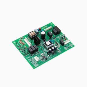
Automatic washing machine control panel PCBA manufacturer pcb circuit board assembly
Read more -
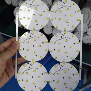
Led pcba solutions aluminium pcb assembly services
Read more -
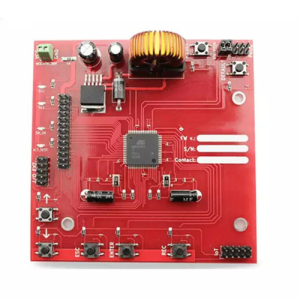
OEM Electronic Fire Alarm Control Panel PCBA Circuit Board
Read more -
OEM/ODM Fire Alarm System Control Panel PCB Board
Read more -
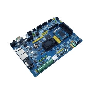
Pcb assembling Printed circuit board assembly manufacturer
Read more -
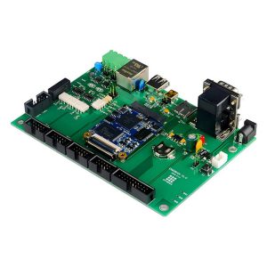
PCBA manufacturing printed circuit board assembly
Read more -
Pressure Sensor Medical Electronic Care Device PCB Board Assembly
Read more -

Professional Custom PCB and PCBA manufacturer PCB Electronic Board Assembly
Read more -
Shenzhen OEM Electronic Copying Pcb Manufacturing Assembly Design Service PCBA One Stop Factory
Read more