
Description
FR4 Multilayer PCB Manufacturer
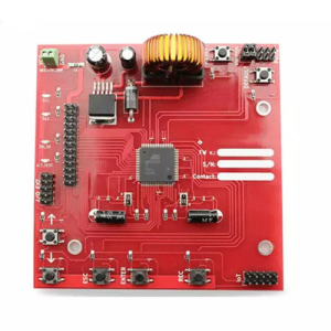
AVPCB provides custom FR4 multilayer PCB manufacturing for prototypes, engineering builds and volume production. Our multilayer PCB capabilities cover standard FR4 and High-Tg FR4 boards, with support for complex structures including blind and buried vias, via-in-pad, HDI designs and controlled impedance.
We currently support PCB designs of up to 36 layers, with minimum line width and spacing down to 3/3 mil, minimum hole sizes down to 0.1 mm, and copper weights up to 12 oz depending on the board structure and manufacturing requirements.
Whether you need a conventional 4-layer control PCB or a higher-layer-count board for industrial, communication, medical or automotive electronics, our engineering team can review your Gerber files, stackup, material requirements and fabrication specifications before production.
FR4 Multilayer PCB Manufacturing Capabilities
Our multilayer PCB manufacturing capabilities are designed to support both standard and technically demanding FR4 designs.
| Parameter | Manufacturing Capability |
|---|---|
| Layer Count | 1–36 Layers |
| Base Material | FR4, High-Tg FR4, Isola and other materials upon request |
| Minimum Line / Space | 3 / 3 mil |
| Minimum Hole Size | 0.1 mm |
| Copper Weight | Up to 12 oz |
| Via Options | Through Hole, Blind Via, Buried Via, Via-in-Pad |
| Advanced PCB Structures | HDI, Half Holes and complex multilayer structures |
| Controlled Impedance | Available |
| Surface Finish | ENIG, HASL, OSP and other options |
| Solder Mask Colors | Green, Blue, Black, Yellow, Red, White, Purple |
| Production Support | Prototype and Volume Production |
Actual manufacturing limits may vary depending on layer count, board thickness, copper weight, via structure and material selection. Send us your PCB files and specifications for a manufacturability review.

FR4 Material Options for Multilayer PCBs
FR4 remains one of the most widely used PCB base materials because it offers a practical balance of electrical insulation, mechanical strength, dimensional stability and manufacturing flexibility.
AVPCB supports different FR4 material options according to operating temperature, reliability requirements and circuit complexity.
Standard FR4
Standard FR4 is suitable for a wide range of general-purpose multilayer PCB applications, including industrial controls, consumer electronics, power control systems and communication equipment.
It is commonly selected when the application does not require unusually high operating temperatures or specialized thermal performance.
High-Tg FR4
High-Tg FR4 can be selected for applications that require improved thermal resistance and dimensional stability.
It is often considered for:
- Higher-layer-count multilayer PCBs
- Multiple lead-free reflow cycles
- Automotive electronics
- Industrial control equipment
- Power electronics
- High-reliability electronic assemblies
The appropriate Tg grade should be selected according to the operating environment, assembly process and expected thermal loading.
Specific Laminate Requirements
If your design specifies a particular laminate manufacturer, material family or electrical property, provide the material information with your PCB files.
Our engineering team can review material availability and recommend suitable alternatives when necessary.
Multilayer PCB Stackup Options
The stackup is one of the most important parts of a multilayer PCB design.
A well-designed stackup helps control signal integrity, impedance, power distribution, electromagnetic interference and overall board manufacturability.
A typical multilayer PCB may contain:
- Signal layers
- Ground planes
- Power planes
- Copper foil
- Prepreg
- FR4 core materials
Typical 4-Layer FR4 PCB Stackup
A common 4-layer structure may use:
Layer 1 – Signal
Layer 2 – Ground Plane
Layer 3 – Power / Signal Plane
Layer 4 – Signal
This configuration provides better signal reference and power distribution than a conventional double-sided PCB.
Higher-Layer-Count Designs
For 6-layer, 8-layer, 10-layer and higher-layer-count PCBs, additional signal and reference planes can be introduced according to routing density and electrical requirements.
AVPCB can review your proposed stackup based on factors such as:
- Finished board thickness
- Layer count
- Copper thickness
- Impedance targets
- Signal routing requirements
- Via structure
- Material type
- Power and ground plane requirements
If you do not have a finalized stackup, you can provide your design requirements for engineering review before production.
Via and Interconnection Options
Multilayer PCBs may require different via structures depending on component density and routing complexity.
Through-Hole Vias
Through-hole vias pass through the complete PCB stack and provide electrical connections between multiple layers.
They are widely used in conventional multilayer PCB designs due to their mature manufacturing process and good reliability.
Blind Vias
Blind vias connect an outer layer to one or more internal layers without passing through the entire PCB.
They can help increase routing density and reduce the amount of board space occupied by conventional through vias.
Buried Vias
Buried vias are located completely inside the multilayer PCB and connect internal copper layers.
They are commonly used when additional routing space is required on the outer layers.
Via-in-Pad
Via-in-pad technology places the via directly within a component pad.
This design can be useful for high-density component layouts, fine-pitch devices and BGA packages where available routing space is limited.
HDI Structures
For high-density PCB designs, AVPCB can support HDI-related structures according to the design requirements.
HDI technology can help accommodate:
- Fine-pitch components
- Dense BGA packages
- Compact PCB layouts
- Higher connection density
- Shorter interconnection paths
The exact via structure should be reviewed together with the stackup and fabrication requirements.
Copper Weight and Surface Finish Options
Copper thickness has a direct influence on current carrying capacity, thermal performance and manufacturing complexity.
AVPCB supports copper weights up to 12 oz for suitable PCB structures.
For most conventional multilayer PCBs, lower copper weights are more common, while heavier copper may be required for power electronics, industrial controls and high-current circuits.
Available surface finish options include:
- ENIG
- HASL
- OSP
- Other finishes according to project requirements
The appropriate surface finish depends on component type, assembly process, storage requirements, solderability and product reliability requirements.
Why Use FR4 Multilayer PCBs?
FR4 multilayer PCBs are widely used when circuit complexity exceeds what can be efficiently achieved with single-sided or double-sided boards.
Higher Routing Density
Additional copper layers allow designers to route more signals within a limited PCB area.
This makes multilayer boards suitable for compact electronic systems with a large number of connections.
Dedicated Power and Ground Planes
Multilayer structures allow dedicated power and ground planes to be incorporated into the PCB stackup.
This can improve power distribution and provide more stable reference planes for signal routing.
Improved Signal Integrity
A carefully designed stackup can provide better signal return paths and controlled impedance structures for high-speed signals.
Smaller PCB Size
By moving part of the routing to internal layers, designers can reduce PCB area while maintaining circuit complexity.
Flexible Layer Configuration
FR4 multilayer PCBs can be designed with different combinations of signal, power and ground layers according to electrical and mechanical requirements.
Controlled Impedance Multilayer PCB Manufacturing
Controlled impedance is an important consideration for many high-speed and high-frequency digital circuits.
Impedance is affected by several factors, including:
- Trace width
- Copper thickness
- Dielectric thickness
- FR4 dielectric properties
- Distance to reference planes
- Stackup configuration
For controlled impedance projects, please provide the target impedance values together with your PCB files and stackup requirements.
Our engineering team can review the design before production and confirm whether the proposed structure is suitable for manufacturing.
FR4 Multilayer PCB Manufacturing Process
Multilayer PCB manufacturing requires accurate alignment and controlled processing of multiple internal and external copper layers.
A typical production process includes:
1. Material Preparation
FR4 cores, copper foil and prepreg materials are prepared according to the approved stackup and material requirements.
2. Inner-Layer Imaging and Etching
Circuit patterns are transferred to the inner copper layers and unwanted copper is removed through etching.
3. Inner-Layer Inspection
The internal circuits are inspected before lamination to identify opens, shorts or pattern defects.
4. Layup and Multilayer Lamination
Inner layers, prepreg and copper foil are aligned and laminated under controlled temperature and pressure to form the multilayer structure.
5. Drilling
Mechanical or other appropriate drilling processes are used to create through holes, vias and component holes according to the PCB design.
6. Hole Metallization
The drilled holes are prepared and metallized to establish electrical connections between copper layers.
7. Outer-Layer Circuit Formation
The external circuit patterns are formed through imaging, plating and etching processes.
8. Solder Mask and Silkscreen
Solder mask protects the copper circuitry, while silkscreen identifies component positions and other markings.
9. Surface Finish
The required surface finish, such as ENIG, HASL or OSP, is applied according to the project specifications.
10. Profiling
Boards are routed, V-scored or otherwise processed to the required final dimensions.
11. Electrical Testing and Final Inspection
Finished PCBs undergo electrical and visual inspections before shipment.
Quality Control for Multilayer PCBs
Quality control is especially important for multilayer boards because many critical features are located inside the PCB and cannot be visually inspected after lamination.
Our manufacturing and inspection process focuses on key areas including:
- Inner-layer circuit integrity
- Layer alignment
- Lamination quality
- Drilling accuracy
- Hole wall plating
- Copper pattern quality
- Solder mask quality
- Surface finish
- Electrical continuity
- Finished dimensions
Available inspection and testing methods are selected according to the PCB structure and customer requirements.
For technically demanding projects, provide any specific testing or acceptance requirements together with the production files.
Applications of FR4 Multilayer PCBs
FR4 multilayer PCBs are used across a wide range of electronic industries.
Industrial Control
Used in PLCs, industrial controllers, automation systems, monitoring equipment and factory electronics requiring multiple signal and power connections.
Telecommunications
Suitable for communication equipment, network devices and control systems where routing density and signal integrity are important.
Automotive Electronics
Multilayer PCBs can be used in electronic control systems, power management systems and other automotive electronic modules according to the required material and reliability specifications.
Medical Electronics
Used in medical electronic equipment where compact layouts, stable electrical performance and consistent manufacturing are required.
IoT Devices
Multilayer structures help accommodate processors, sensors, communication modules and power circuits in compact IoT products.
Power Electronics
Heavy copper and multilayer structures can support applications involving higher current, power distribution and industrial power control.
Consumer Electronics
Compact multilayer PCBs are widely used in electronic devices that require high component density within limited space.
Prototype to Volume Production
AVPCB supports both prototype multilayer PCB fabrication and volume production.
Prototype production can be used to verify:
- Circuit design
- Stackup
- Mechanical dimensions
- Assembly compatibility
- Electrical performance
- Product functionality
After the design has been validated, the same project can move toward larger production quantities according to your purchasing requirements.
For repeat orders, providing consistent PCB files, fabrication notes and approved specifications helps maintain production consistency.
Custom FR4 Multilayer PCB Manufacturing
Different applications require different PCB structures.
AVPCB can review custom requirements including:
- Layer count
- PCB dimensions
- Finished board thickness
- Copper weight
- FR4 material
- Tg requirement
- Blind and buried vias
- Via-in-pad
- Controlled impedance
- Surface finish
- Solder mask
- Silkscreen
- Special routing or mechanical features
Instead of selecting a standard PCB configuration only by layer count, we recommend evaluating the complete stackup and manufacturing requirements together.
What to Send for an FR4 Multilayer PCB Quote
For faster engineering review and quotation, please provide as much of the following information as possible:
- Gerber files
- Drill files
- Layer count
- PCB dimensions
- Finished thickness
- Copper weight
- FR4 material or Tg requirement
- Surface finish
- Solder mask color
- Controlled impedance requirements
- Blind / buried via requirements
- Quantity
- Special testing requirements
- Any critical fabrication notes
If some specifications have not yet been finalized, send your existing PCB design files and requirements. Our team can review the manufacturing information with you before quotation.
FR4 Multilayer PCB FAQs
How many layers can AVPCB manufacture?
AVPCB currently supports FR4 multilayer PCB manufacturing with up to 36 layers, depending on the board structure, material, copper thickness and other fabrication requirements.
What is the minimum line width and spacing?
Our current manufacturing capability supports minimum line width and spacing down to 3/3 mil for suitable PCB designs.
What is the minimum hole size?
Minimum hole size can reach 0.1 mm, subject to PCB thickness, via structure and design requirements.
Can you manufacture blind and buried via multilayer PCBs?
Yes. AVPCB supports blind vias, buried vias, via-in-pad and HDI-related structures according to the PCB design.
Do you support High-Tg FR4?
Yes. Standard FR4 and High-Tg FR4 options are available. Material selection should be based on operating temperature, assembly requirements and product reliability requirements.
Can you manufacture heavy copper multilayer PCBs?
AVPCB supports copper weights of up to 12 oz for suitable PCB structures. Heavy copper capability depends on layer configuration, trace geometry and overall board design.
Can you provide controlled impedance PCBs?
Yes. Controlled impedance manufacturing is available. Please provide your impedance requirements, stackup information or design files for engineering review.
Do you support both prototypes and mass production?
Yes. We support FR4 multilayer PCB projects from prototype quantities through volume production.
Request Your FR4 Multilayer PCB Quote
Need a custom multilayer PCB with specific layer count, FR4 material, copper weight, via structure or controlled impedance?
Send your Gerber files and PCB specifications to AVPCB for a manufacturability review and quotation.